- 您现在的位置:买卖IC网 > Sheet目录3851 > PIC16F88-I/ML (Microchip Technology)IC MCU FLASH 4KX14 EEPROM 28QFN
110
8008H–AVR–04/11
ATtiny48/88
12.11 Register Description
12.11.1
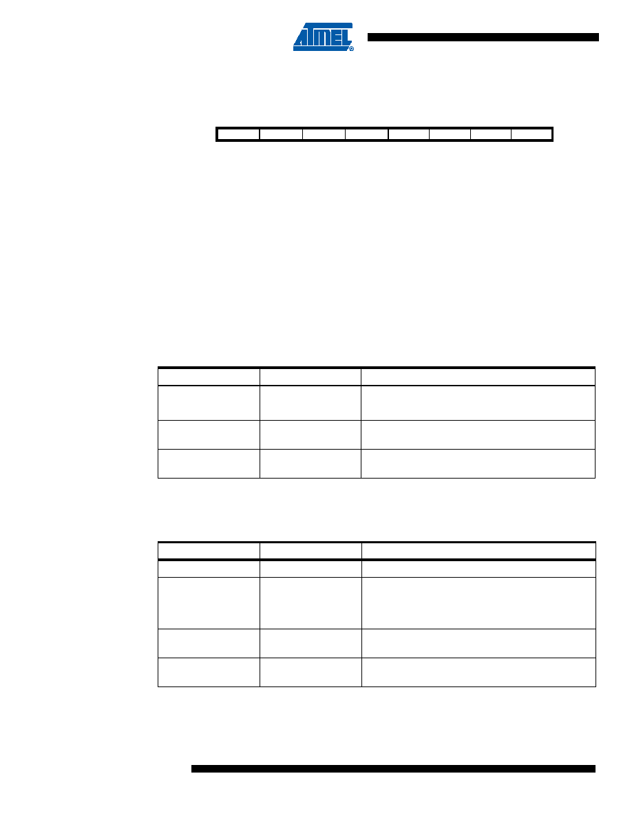
TCCR1A – Timer/Counter1 Control Register A
Bits 7:6 – COM1A[1:0]: Compare Output Mode for Channel A
Bits 5:4 – COM1B[1:0]: Compare Output Mode for Channel B
The COM1A[1:0] and COM1B[1:0] control the Output Compare pins (OC1A and OC1B respec-
tively) behavior. If one or both of the COM1A[1:0] bits are written to one, the OC1A output
overrides the normal port functionality of the I/O pin it is connected to. If one or both of the
COM1B[1:0] bit are written to one, the OC1B output overrides the normal port functionality of the
I/O pin it is connected to. However, note that the Data Direction Register (DDR) bit correspond-
ing to the OC1A or OC1B pin must be set in order to enable the output driver.
When the OC1A or OC1B is connected to the pin, the function of the COM1x[1:0] bits is depen-
dent of the WGM1[3:0] bits setting. Table 12-2 shows the COM1x[1:0] bit functionality when the
WGM1[3:0] bits are set to a Normal or a CTC mode (non-PWM).
Table 12-3 shows the COM1x[1:0] bit functionality when the WGM1[3:0] bits are set to the fast
PWM mode.
Note:
1. A special case occurs when OCR1A/OCR1B equals TOP and COM1A1/COM1B1 is set. In
this case the compare match is ignored, but the set or clear is done at TOP. See “Fast PWM
Mode” on page 101. for more details.
Bit
7654
3
2
1
0
COM1A1
COM1A0
COM1B1
COM1B0
–
WGM11
WGM10
TCCR1A
Read/Write
R/W
R
R/W
Initial Value
0000
0
Table 12-2.
Compare Output Mode, non-PWM
COM1A1/COM1B1
COM1A0/COM1B0
Description
0
Normal port operation, OC1A/OC1B disconnected.
0
1
Toggle OC1A/OC1B on Compare Match.
10
Clear OC1A/OC1B on Compare Match (Set output to
low level).
11
Set OC1A/OC1B on Compare Match (Set output to
high level).
Table 12-3.
Compare Output Mode, Fast PWM(1)
COM1A1/COM1B1
COM1A0/COM1B0
Description
0
Normal port operation, OC1A/OC1B disconnected.
01
WGM1[3:0] = 14 or 15: Toggle OC1A on Compare
Match, OC1B disconnected (normal port operation).
For all other WGM1 settings, normal port operation,
OC1A/OC1B disconnected.
10
Clear OC1A/OC1B on Compare Match, set
OC1A/OC1B at TOP
11
Set OC1A/OC1B on Compare Match, clear
OC1A/OC1B at TOP
发布紧急采购,3分钟左右您将得到回复。
相关PDF资料
PIC18F26J53-I/ML
IC PIC MCU 64KB FLASH 28QFN
PIC18F46K80-I/ML
MCU PIC 64KB FLASH 44QFN
PIC32MX130F064D-I/TL
IC MCU 32BIT 64KB FLASH 44-VTLA
PIC32MX130F064D-I/ML
IC MCU 32BIT 64KB FLASH 44-QFN
PIC18LF46K80-I/ML
MCU PIC ECAN 64KB FLASH 44QFN
AT89S51-24JI
IC 8051 MCU 4K FLASH 44PLCC
AT89S51-24JC
IC 8051 MCU 4K FLASH 44PLCC
AT89S51-24AI
IC 8051 MCU 4K FLASH 44TQFP
相关代理商/技术参数
PIC16F88-I/ML
制造商:Microchip Technology Inc 功能描述:8BIT FLASH MCU SMD 16F88 QFN-28
PIC16F88-I/P
功能描述:8位微控制器 -MCU 7KB 368 RAM 16 I/O RoHS:否 制造商:Silicon Labs 核心:8051 处理器系列:C8051F39x 数据总线宽度:8 bit 最大时钟频率:50 MHz 程序存储器大小:16 KB 数据 RAM 大小:1 KB 片上 ADC:Yes 工作电源电压:1.8 V to 3.6 V 工作温度范围:- 40 C to + 105 C 封装 / 箱体:QFN-20 安装风格:SMD/SMT
PIC16F88-I/P
制造商:Microchip Technology Inc 功能描述:IC 8BIT FLASH MCU 16F88 DIP18
PIC16F88-I/SL
制造商:Microchip Technology Inc 功能描述:
PIC16F88-I/SO
功能描述:8位微控制器 -MCU 7KB 368 RAM 16 I/O RoHS:否 制造商:Silicon Labs 核心:8051 处理器系列:C8051F39x 数据总线宽度:8 bit 最大时钟频率:50 MHz 程序存储器大小:16 KB 数据 RAM 大小:1 KB 片上 ADC:Yes 工作电源电压:1.8 V to 3.6 V 工作温度范围:- 40 C to + 105 C 封装 / 箱体:QFN-20 安装风格:SMD/SMT
PIC16F88-I/SO
制造商:Microchip Technology Inc 功能描述:8BIT FLASH MCU SMD 16F88 SOIC18
PIC16F88-I/SOG
功能描述:8位微控制器 -MCU 7KB 368 RAM 16 I/O Lead Free Package RoHS:否 制造商:Silicon Labs 核心:8051 处理器系列:C8051F39x 数据总线宽度:8 bit 最大时钟频率:50 MHz 程序存储器大小:16 KB 数据 RAM 大小:1 KB 片上 ADC:Yes 工作电源电压:1.8 V to 3.6 V 工作温度范围:- 40 C to + 105 C 封装 / 箱体:QFN-20 安装风格:SMD/SMT
PIC16F88-I/SS
功能描述:8位微控制器 -MCU 7KB 368 RAM 16 I/O RoHS:否 制造商:Silicon Labs 核心:8051 处理器系列:C8051F39x 数据总线宽度:8 bit 最大时钟频率:50 MHz 程序存储器大小:16 KB 数据 RAM 大小:1 KB 片上 ADC:Yes 工作电源电压:1.8 V to 3.6 V 工作温度范围:- 40 C to + 105 C 封装 / 箱体:QFN-20 安装风格:SMD/SMT